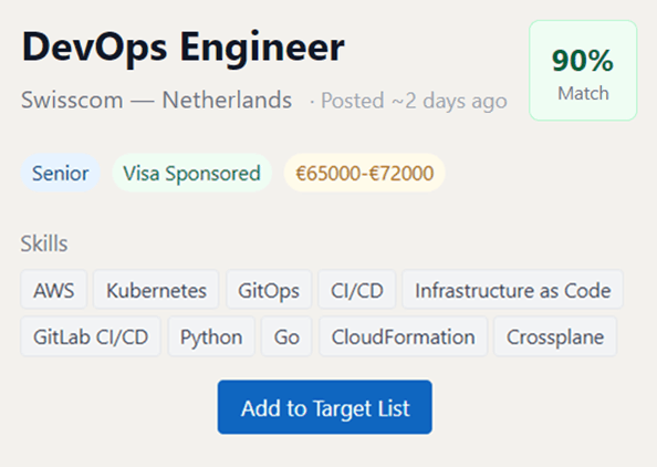
GaN Process Development Engineer

X Fab — Germany · Posted ~2 hours ago

Mid Full-time Onsite

Skills

GaN semiconductor devices Wide Band Gap technology Semiconductor process development TCAD simulation Design of Experiments Electrical characterization GaN TCAD Semiconductor processes

🔓 Log in to save this job, tailor your resume & track your apply process — 7 days free, no card needed.

Log in to add to target list

Summary ✨ AI‑Generated

A semiconductor technology organization is looking for an engineer to develop next-generation wide band gap devices and manufacturing processes. The role includes simulation, experimental design, device testing, and collaboration with multidisciplinary teams.

Highlights

Opportunity to work on advanced semiconductor technologies within an international engineering environment and contribute to device innovation.

Description

Dresden, Germany X-FAB is looking for a GaN / Wide Band Gap device and process development engineer to join our global Process Development team, in Dresden, Germany, but working as part of an international organization developing Wide Band Gap technologies. Your Pitch › Development of GaN / Wide Band Gap semiconductor devices and processes. › Define semiconductor process flows and device architectures. › TCAD simulation of devices and processes. › Definition, implementation and evaluation of experiments using Design of Experiments (DoE) methodology. › Development and design of test structures. › Electrical characterization of GaN / Wide Band Gap devices. › Process integration and cooperation with other departments within X-FAB. › Offer technical support to customers. › Cooperation with external partners. › Management of development projects, working in interdisciplinary and international teams. Your Profile › Master’s degree in the field of electrical engineering, microelectronics or related fields. › Minimum 3 years of experience in development, functionality, manufacturing, characterization and application of GaN / Wide Band Gap semiconductor devices. › Experience with GaN / Wide Band Gap wafer processes. › Experience in the development environment for the automotive industry is desirable. › Enjoy teamwork in a multicultural work environment. › Interest in the development of modern semiconductor devices with the highest quality standards. › Project management experience. › Strong communication skills in an international environment. Contact person : Mathilde Stenzel Apply now Back to list Your Benefits Of Applying Without a Profile Easy application without any registrationOnly contact details and CV are required and voluntary attachment uploadTakes only 3 minutes Apply without profile Your Benefits Of Creating a Profile Create your convincing applicant profileTrack your application status regularlySave your application and continue at any timeTakes only 10 minutes Apply with profile